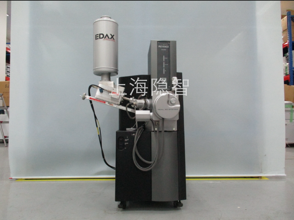
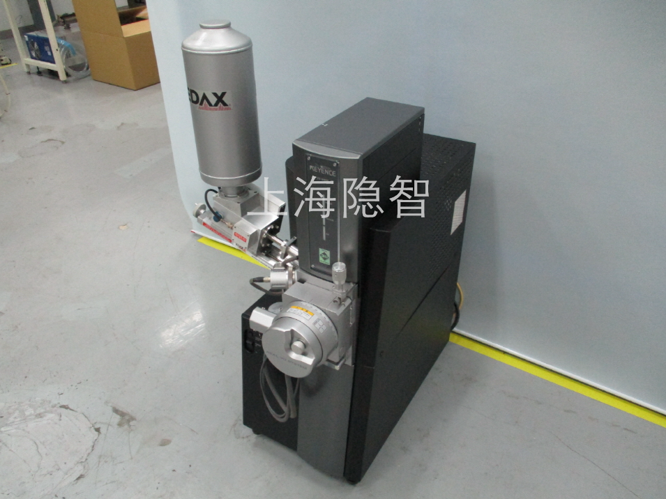
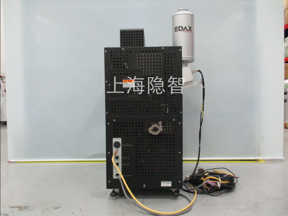
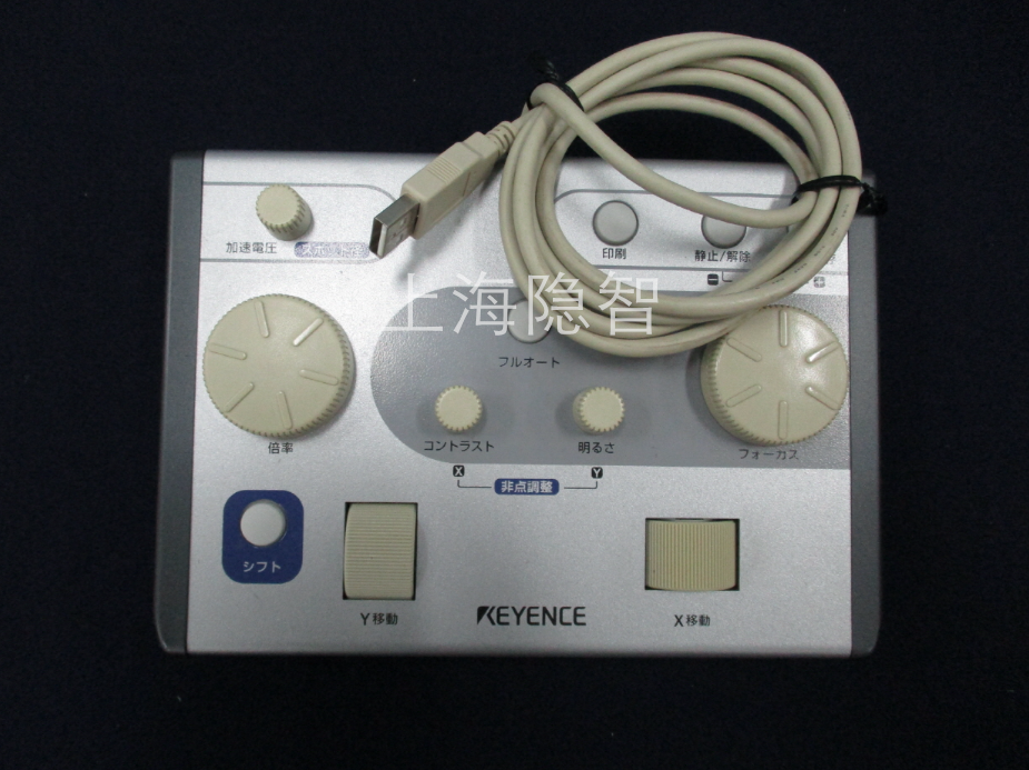
KEYENCE 3D Surface Measurement Microscope VE-9800
The KEYENCE VE-9800 is a high-precision 3D surface measurement microscope that utilizes advanced optical technology and image processing algorithms to achieve nanometer-level surface topography measurements. This system is widely used in semiconductor, electronic components, precision machinery, and materials science fields, providing accurate measurement solutions for surface roughness, step height, and micro-topography parameters.
Price:Negotiable
Service charge: 10% of the transaction price
- 设备品牌:Keyence
- 设备安装时间:2006
- 设备所在地:
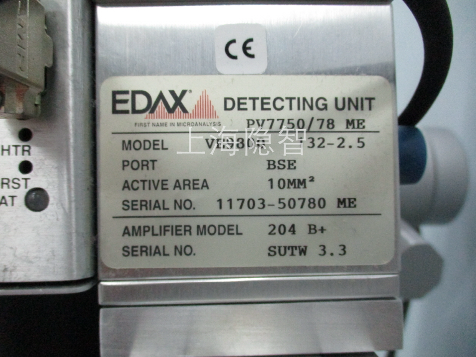
- 设备型号:VE-9800
- 设备序列号:1170350780
- 电压:
- 电频:
- 尺寸:
- 重量:
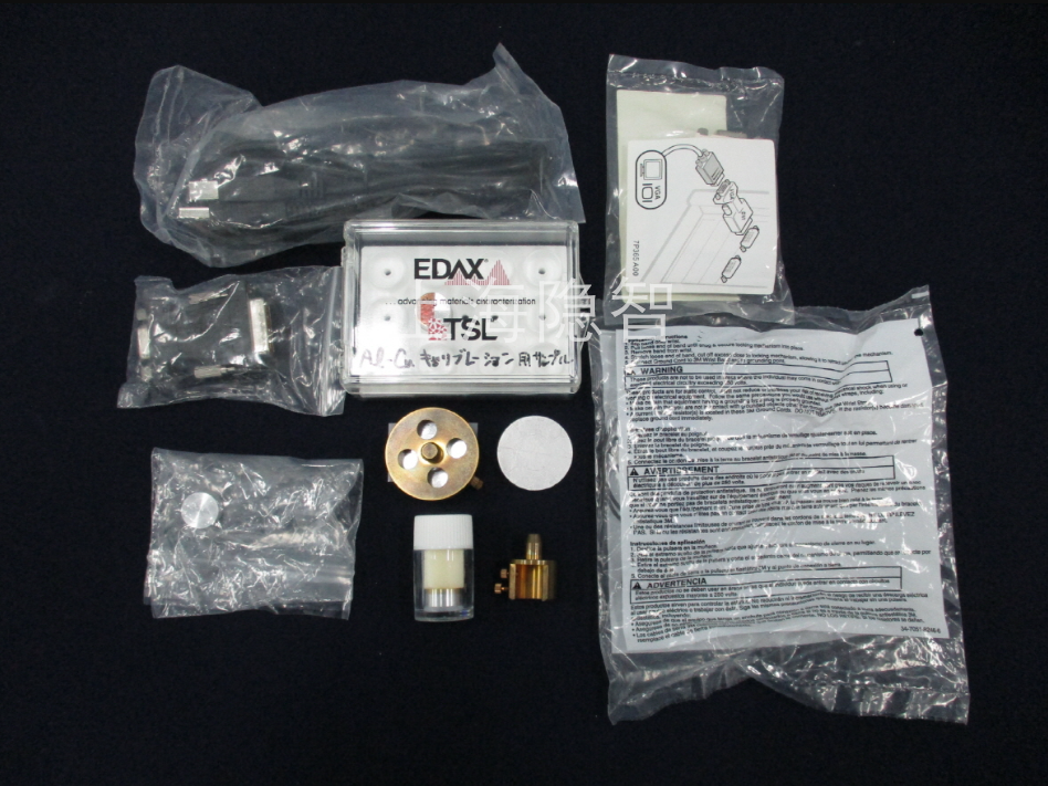
Device built-in
KEYENCE 3D Surface Measurement Microscope VE-9800 - English Introduction
Product Overview
The KEYENCE VE-9800 is a high-precision 3D surface measurement microscope that utilizes advanced optical technology and image processing algorithms to achieve nanometer-level surface topography measurements. This system is widely used in semiconductor, electronic components, precision machinery, and materials science fields, providing accurate measurement solutions for surface roughness, step height, and micro-topography parameters.
Core Technical Features
- Ultra-High Resolution Measurement System
- Employs white light interferometry with vertical resolution up to 0.1nm and horizontal resolution of 0.5μm
- Equipped with high-precision piezoelectric displacement stage for nanometer-level Z-axis positioning accuracy
- Supports continuous zoom observation from 10x to 2000x magnification
- Intelligent Measurement Capabilities
- Auto-focus and automatic measurement functions significantly improve efficiency
- Supports multiple measurement modes including multi-point measurement, line roughness, and area roughness analysis
- Built-in library of 200+ ISO/JIS standard parameters to meet various industry requirements
- Advanced Image Processing Technology
- Proprietary interference fringe analysis algorithm effectively eliminates environmental vibration effects
- Real-time 3D rendering for immediate surface topography visualization
- Supports advanced analysis functions including surface texture analysis and profile extraction
Typical Applications
- Semiconductor Industry: Wafer surface defect inspection, photoresist thickness measurement
- Precision Manufacturing: Cutting tool edge wear analysis, mechanical component surface quality inspection
- Materials Research: Thin film thickness measurement, coating surface topography analysis
- Electronic Components: PCB trace height measurement, solder joint 3D morphology inspection
System Advantages
- User-Friendly Operation: Intuitive interface with highly automated measurement workflows
- Measurement Stability: Vibration-resistant design ensures >99% measurement repeatability
- Comprehensive Data Output: Generates complete datasets including 2D/3D images, cross-sectional profiles, and roughness parameters
- High Expandability: Supports integration with automation equipment for batch inspection
Conclusion
The KEYENCE VE-9800, with its nanometer-level measurement accuracy, intelligent operation, and powerful analysis capabilities, has become the ideal tool for micro/nano-scale surface measurement. Whether for quality analysis in R&D laboratories or process control in production lines, it delivers reliable measurement data to help users improve product quality and production efficiency.